PRODUCTION OF SI SINGLE CRYSTALS
Crystal growing with the Czochralski process
Principle of the Czochralski process
In the Czochralski process, a cylindrical silicon single crystal is grown from a
Si melt as shown schematically in the figure below
. For this purpose, polycrystalline silicon (e.g.
originating from the Siemens process) is first melted together with dopants in
a quartz crucible above 1400°C in an inert gas atmosphere (e.g.
argon). The quartz crucible sits flush in a
graphite crucible, which, due to its very high thermal conductivity, transfers the
temperature of the heating wall evenly to the quartz crucible.
In
this Si melt, which is now held close to the melting point of silicon
, a Si single crystal ("seed crystal" or "seed") is immersed. "seed crystal" or "seed ring") of the
desired crystal orientation (e.g. <100>, <110> or
<111>), on which the molten silicon begins to crystallise through the heat dissipation via
the seed ring. The seed ring is slowly
pulled out of the melt, whereby the growing crystal and the crucible
rotate in opposite directions to optimise the homogeneity of the crystal and its doping
. The pulling speed of typically several
cm/hour determines the diameter
of the growing Si cylinder, which is kept as constant as possible.
Before the end of crystal growth,
its diameter is continuously reduced to zero by increasing the pulling speed
in order to avoid thermal stresses in the crystal
due to abrupt lifting from the melt.
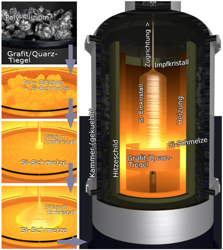
The various steps involved in pulling Si single crystals using the Czochralski process: Melting of polycrystalline silicon with dopants, immersion of the seed crystal, and pulling of the single crystal.
Advantages and disadvantages of the Czochralski process
The advantages of the Czochralski process are large possible
crystal diameters (currently up to 18 inches=46 cm) and - compared to
the float zone process explained in the next section - lower
costs of the wafers produced from it.
One disadvantage of the Czochralski process is contamination through the crucible wall with oxygen (approx. 1018 cm-3), carbon (approx. 1017 cm-3)
and metals, which reduce the minority lifetime in the silicon
. Another disadvantage is the relatively uneven
doping over the entire crystal volume, which means that uniformly
very lightly doped, high-resistance CZ wafers with resistances over approx.
100 Ohm cm are not possible. A magnetic field at the location of the melt ("Magnetic
Czochralski", MCZ) can suppress non-stationary currents in the melt
, which significantly improves the homogeneity of the
dopant concentration built into the crystal and thus makes high-resistance CZ wafers
possible.
Crystal growing with the float zone method
Principle of the float zone process
In the float zone (FZ) or zone melting process, a monocrystalline
silicon seed crystal
is brought into contact with a polycrystalline Si cylinder, as shown schematically in the figure at
below. Starting from
this point, an induction coil melts the poly-silicon in
a spatially limited zone. During cooling
the melt crystallises and assumes the crystal orientation
(e.g. <100>, <110> or <111>) of the seed.
When incorporated into the resulting crystal lattice
, impurities are energetically disadvantaged compared to silicon (lower chemical
potential), so that they accumulate in the melt and, after
completion of the zone melting process, are concentrated
at the end of the crystal, where they can be separated. Doping takes place via
phosphine (PH3), arsine (AsH3) or diborane (B2H6) added to the inert gas atmosphere.
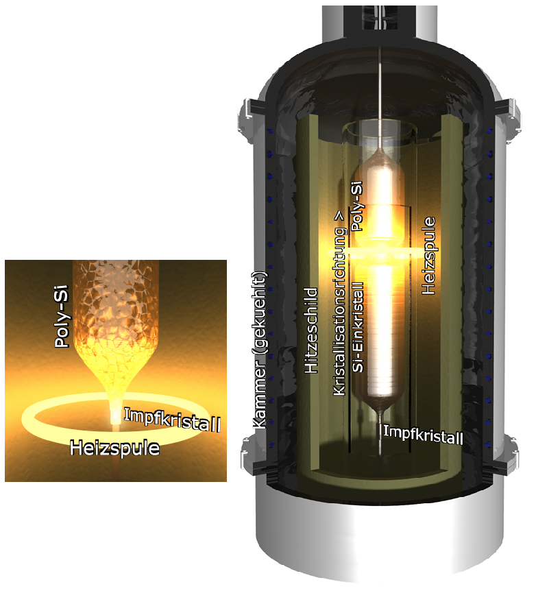
Schematic of the zone melting process: After a Si single crystal is melted onto a poly-Si cylinder (top), it takes on the crystal direction of the seed along the length through melting and crystallisation.
Advantages and disadvantages of the float zone process
The main advantage of the float zone process is the possibility of specifying the
dopant concentration at a very low level with high
homogeneity, which makes it possible to realise very high-resistance (1,000 - 10,000 ohm cm)
and very narrowly specified wafers in terms of resistance
. In addition, contamination with foreign substances is much lower
(oxygen and carbon < 1016 cm-3) than with the CZ process, as the
Si melt
does not come into contact with quartz and no graphite crucibles are used
. One disadvantage of the FC process is the relatively high cost,
typically three to
four times the cost of the finished wafer compared to the Czochralski process. For technical reasons,
the diameter of the single crystal is limited and the current
state of the art allows a maximum of eight-inch diameter FZ wafers.
Further Information:
> Application areas and compatibilities
> Image Reversal Resist Processing
Filter products
