FROM QUARTZ SAND TO HIGH-PURITY SILICON
Origin and occurrence of silicon
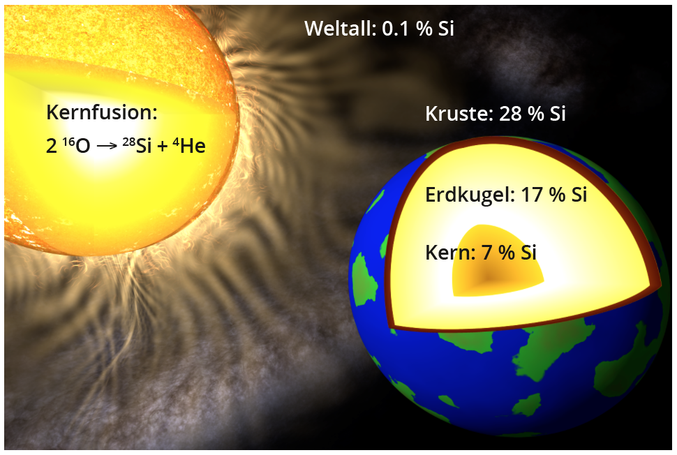
Silicon fuses from oxygen nuclei in the interior of massive suns at temperatures above109 K and is hurled into space at the end of the star's life in supernova explosions. Of the hydrogen and helium-dominated visible matter in the universe , silicon makes up less than 0.1 % of the total mass.

The abundance (in mass %) of silicon in the entire universe, the globe, the earth's crust and the earth's core.
In our solar system, which was formed from the "ashes" of earlier stellar explosions, silicon has mainly accumulated in the inner planets, which have lost most of their volatile elements due to their proximity to the central sun. In the entire globe, silicon is the third most common element after iron and oxygen at approx. 17 %, closely followed by magnesium. In the Earth's core, which consists mainly of iron, silicon is in second place with approx. 7 %. The approx. 40 km thick earth's crust contains around 28 % silicon in the form of silicate minerals or quartz (SiO2) as the second most common element after oxygen, as well as dissolved as silicic acid (Si(OH)4) in the world's oceans. In contrast, the natural deposits of solid, i.e. elemental, silicon do not play a role in terms of quantity.
Production and use of raw silicon
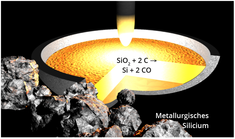
To produce elemental silicon, quartz sand (SiO2) is reduced in smelting reduction furnaces at approx. 2000°C with carbon to raw silicon (also known as metallurgical silicon) with a purity of approx. 98 - 99%, or significantly higher through the use of purer starting materials and electrodes (Fig. below). The majority of global production, which mainly takes place in China and Russia (approx. 7 million tonnes in 2014), is used as an alloying component for steels and aluminium and as a starting material for the production of silicones. Only around 2 % of raw silicon is processed into hyperpure silicon as described in the following section , of which around 90 % is used to manufacture silicon solar cells. Finally, a few hundred tonnes per year are used in the production of silicon wafers for the semiconductor sector.

Reduction of SiO2 with carbon to raw silicon in an electric arc furnace.
Processing raw silicon into hyperpure silicon
The concentration of impurities in raw silicon
is still many orders of magnitude too high for use as a semiconductor in microelectronics or
photovoltaics. In order to achieve the required
electronic properties, the raw silicon must therefore be "refined" into
hyperpure silicon.
In the first step of this processing into hyperpure silicon, raw silicon is converted at approx. 300°C with HCl into trichlorosilane (HSiCl3) via Si + 3 HCl → HSiCl3 + H2
, whereby many impurities such as iron, which
do not form volatile chlorine compounds at these temperatures,
remain behind. The
trichlorosilane contaminated with other chlorine compounds is brought to a purity level of
up to 99.9999999 % ("9N") by multiple distillation and then thermally decomposed to
polycrystalline silicon. This takes place in the so-called
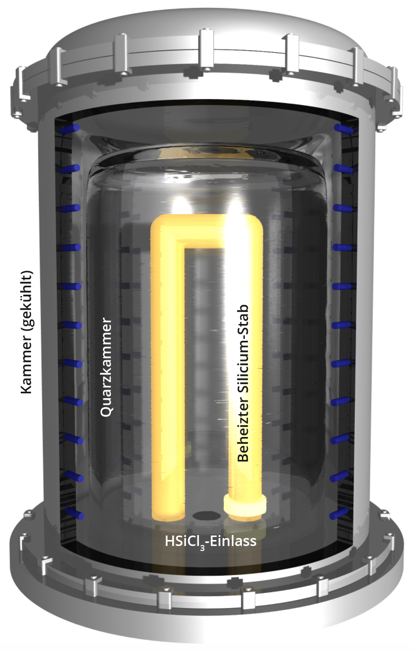
Siemens process (Fig. below): Here, the high-purity trichlorosilane
is heated together with hydrogen on a Si rod heated to approx. 1100°C, the
silicon core via
HSiCl3 + H2 → Si + 3 HCl
to form polycrystalline silicon and HCl, which corresponds to the reverse reaction of trichlorosilane formation.

Conversion of trichlorosilane to polycrystalline silicon on heated Si rods in the so-called Siemens process.
Polycrystalline and monocrystalline silicon
Although the polycrystalline silicon obtained in the Siemens process has a high degree of purity with an impurity concentration of < 1014 cm-3
, it has crystalline grain boundaries,
which form electronic impurities that reduce the efficiency of solar cells manufactured from it
and rule out its use in the field of
microelectronics.
Only monocrystalline silicon can be used as a starting material for the production
of silicon wafers as substrates for microelectronic components,
which is produced from
polycrystalline silicon using the Czochralski or float zone process, as described in the following
sections. In this process, the silicon is also
selectively doped with foreign atoms in order to adjust the electrical
conductivity of the wafers produced from it in a defined manner and homogeneously across the
entire crystal.
Further Information:
> Application areas and compatibilities
> Image Reversal Resist Processing
Filter products


