SILICON WAFER
Material
The ingot from which monocrystalline silicon wafers are produced can be grown using either the Czochralski or float zone process . The inexpensive CZ wafers are by far the most commonly used , while the significantly more expensive FZ wafers are used where substrates with very high resistance (> 100 Ohm cm) and/or minimal impurities from carbon or oxygen are required.
Diameter and shape
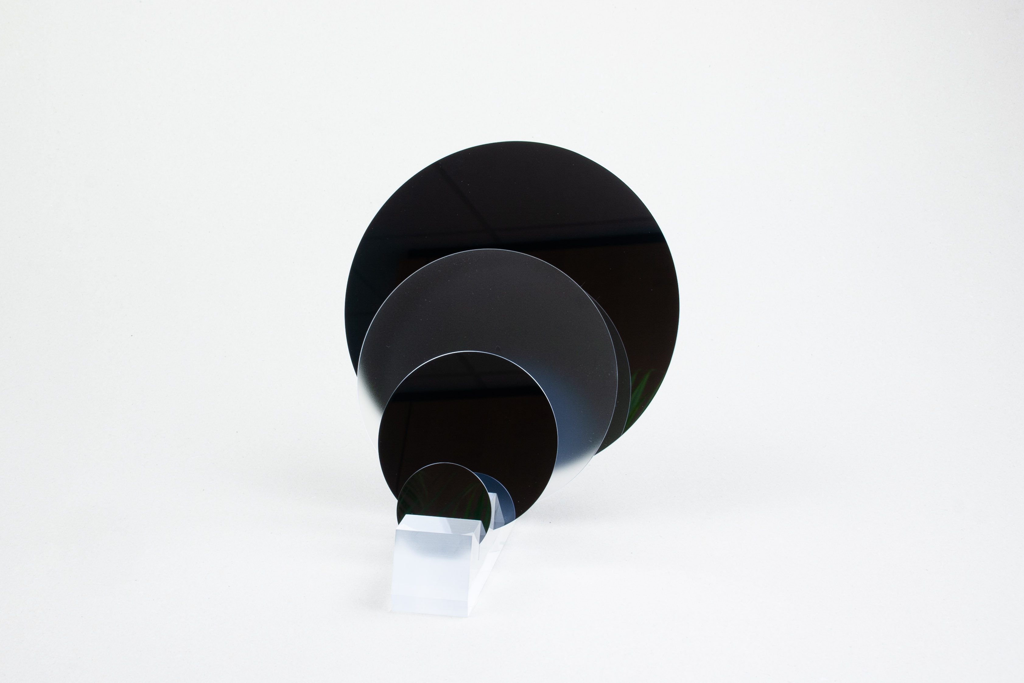
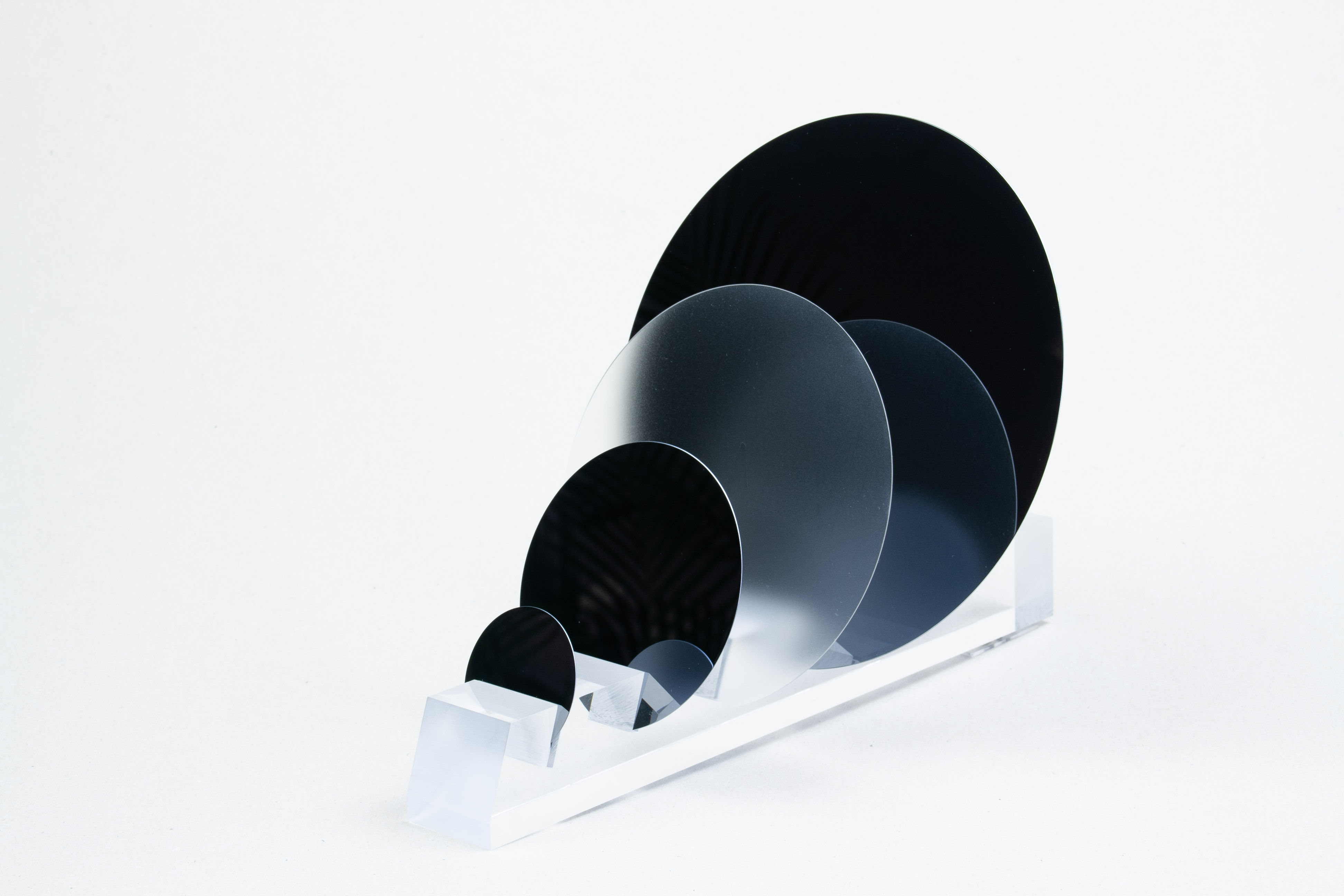
We can offer Si wafers with diameters of 1, 2, 3, 4, 5, 6 and 8 inches . Unless otherwise stated, "inch" in this context only means 25.4 mm for 1 and 2 inch wafers, from 4 inches the diameter is a multiple of 25.0 mm (e.g. 100 mm for 4 inches). In addition to round wafers, wafers separated into rectangular pieces are also possible. Due to the high fixed costs involved in the separation process, from an economic point of view it usually only makes sense to order quantities that correspond to the separation of approx. 25 initial wafers. However, we occasionally keep smaller quantities of separated wafers in stock for more frequently requested quantities.
Orientation and thickness
We can offer silicon wafers in crystal orientation <100> and <111>, <110> orientated wafers may be possible on request . We can only offer wafers tilted against the main crystal directions in exceptional cases and in larger quantities In addition to standard thicknesses depending on the wafer diameter (279 μm at 2 inches, 380 μm at 3 inches, 525 μm at 4 and 5 inches, 675 μm at 6 inches and 725 μm at 8 inches), thinner wafers up to approx. 180 μm are also possible, depending on the diameter. For technological reasons, the upper thickness limit for wafers polished on one or both sides is approx. 2 mm. Thicker wafers or cylinders are possible if the end faces do not have to be ground or polished, in which case the length of the ingot (typically several 10 cm) limits the thickness of the wafer or the length of the cylinder.
Surface
Silicon wafers are usually polished on one or both sides. The roughness (rms) is usually specified to < 1.5 nm or < 1.0 nm, the non-polished side(s) etched to a roughness on a μm scale. In addition to the roughness, the finest polishing marks also define the surface quality of the polished side(s), which is defined by the size S/D (usually 40/20). On request, wafers can also be provided with surfaces "as cut", i.e. without further surface processing steps after sawing.
Prime, test and dummy quality
The specifications for prime and test grade are based on SEMI standards. The price difference is comparatively small, as are the differences in the specifications: Essentially, test-grade wafers have a greater tolerance in the specification of the particles, and occasionally also larger resistance ranges (e.g. 1-20 instead of 1-10 ohm cm). The term "dummy-grade" covers all wafers which, for various reasons, fulfil neither prime-grade nor test-grade requirements. This can simply mean a large thickness tolerance of e.g. +/- 50 μm with otherwise prime-grade-compliant specifications , but also reclaim wafers for which nothing is defined apart from the diameter. Even such wafers are still suitable in many cases for simple coating tests or for testing and running in equipment for wafer processing due to their very favourable price.
Coatings
We also offer our wafers optionally coated over their entire surface with one or several metal films as well as PECVD or LPCVD silicon nitride (stoichiometric or low-stress from thicknesses of several 100 nm) . The thermal double-sided oxidation of silicon wafers is usually carried out dry up to a SiO2 thickness of 200 nm, above this, it is subsequently dry/wet/dry grown in order to combine rapid SiO2 growth with a material quality comparable to dry-grown oxide . SiO2 thicknesses of several μm are possible, but are associated with increasingly high costs as the oxide only grows logarithmically over time.
Further Information:
> Application areas and compatibilities
> Image Reversal Resist Processing


