QUARTZ GLASS WAFER
Material
As explained below, quartz glass is available as JGS1, JGS2 and JGS3 material. The main difference lies in impurities and impurities, which affect the transmission in the short-wave ultraviolet and infrared spectral range.
Diameter and shape
We can offer quartz glass wafers with diameters of 2, 3, 4 and 6 inches . Unless otherwise stated, "inch" in this context means 25.0 mm (and not 25.4 mm), so a 4 inch wafer has a diameter of 100 mm. In addition to round wafers, wafers separated into rectangular pieces are also possible. Due to the high fixed costs involved in the separation process, it usually only makes economic sense to order quantities , which correspond to the separation of approx. 10 initial wafers.
Thickness and surface
Quartz glass wafers are amorphous, which is why no crystal orientation can be defined for the wafers. Common wafer thicknesses are 200 μm, 500 μm, 700 mm and 1000 μm, other thicknesses are possible if necessary. Quartz glass wafers are usually polished on both sides, for certain applications also on one side. The roughness is usually specified at "< 1.5 nm" or "< 1.0 nm".
Production and specifications of quartz glass wafers
Production of fused silica
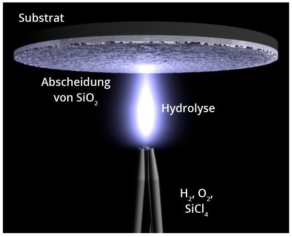
One method for the production of fused silica wafers is the melting and subsequent resolidification of high-purity quartz. Another method is the formation and subsequent oxidation of silicon from gaseous Si-containing starting materials (e.g. from a SiCl4 + H2 + O2 mixture), and subsequent fusion of this "SiO2 dust" to form quartz glass, which has a higher transparency in the deep UV range than fused and resolidified quartz glass produced using this method.
Production of wafers
Wafers are sawn and polished from the resulting blocks, the technical processes for this correspond to those for the production of silicon or quartz wafers.

Schematic representation of the deposition of quartz glass from the gases H2, O2 and SiCl4.
Specifications of quartz glass wafers
JGS1
Ultraviolet Grade Fused Silica
These wafers show
a high transparency in the short-wave spectral range. The transmission
is approx. 90 % in the visible and UV range up to approx. 215 nm and
then drops to values close to 0 % up to approx. 150 nm. In the infrared range
, absorption bands can already be seen from a wavelength of approx. 1.2 μm, which
also have their origin in the relatively high OH concentration of typically 1000 ppm
.
JGS2
Optical Grade Fused Quartz
Compared to JGS1
wafers, the range of high
transmission is shifted towards longer wavelengths in the significantly more favourable JGS2 wafers: The UV absorption
already begins significantly below approx. 270 nm, while in the visible
and IR range the transmission up to approx. 2 μm is above approx. 90 % due to the lower
OH concentration (typically < 300 ppm), i.e.
is essentially only limited by reflection losses.
JGS3
Full Spectrum Fused Silica
These comparatively
expensive wafers exhibit a transmission > 80 % over a large spectral range of approx. 200 nm - 3 μm
due to their very low OH concentration (typ.
< 10 ppm) and close to 90 % in the 250 nm - 2.5 μm range, i.e.
is essentially only limited by reflection losses.
Surface
Quartz glass wafers are usually polished on both sides; a polish on one side is generally possible on request. The roughness of the polished side(s) is usually < 1 nm, a value of < 0.5 nm, which corresponds to almost atomic smoothness, is also technically feasible.
Further Information:
> Application areas and compatibilities
> Image Reversal Resist Processing
Filter products


