GALVANIC APPLICATION EXAMPLES
Microswitch
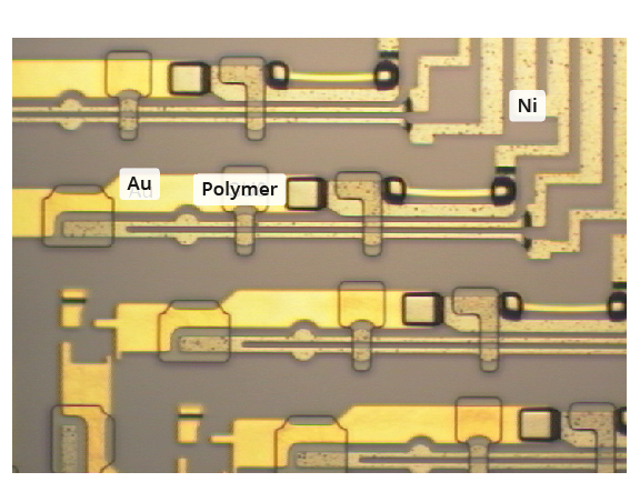
The image above shows a CCD microscope image of a thermal, laterally actuatable, bistable microswitch. The mechanically movable elements consist of approx. 12 µm thick galvanic nickel (electrolyte used: NB Semiplate Ni 100). The smallest dimension of the Ni bars is 4 µm. The contact elements are made of gold (electrolyte: NB Semiplate Au 100). The transparent elements consist of a cross-linked negative varnish and are used for the mechanical connection. The main requirements for electroplating are the avoidance of stress gradients, thickness non-uniformities, particularly with different structure sizes, and the long-term stability of the properties under mechanical and thermal stress. The different levels can be clearly recognised at by the overgrowth of the nickel as a connection to gold structures and the overgrowth of the nickel bars over the edge of the sacrificial layer (made of approx. 4 µm thick Cu, already removed). These different levels place high demands on the coating process (here AZ® 9260).
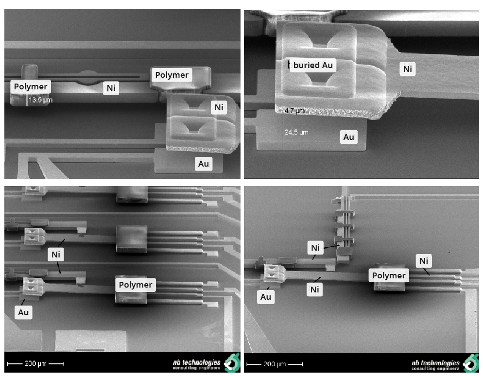
These are several SEM images of a thermal actuator and a contact of a microswitch. Mechanical elements are made of bright nickel (electrolyte: NB Semiplate Ni 100). To achieve vertical deflection, a stress gradient is set in the nickel layer using the deposition parameters . The stability of the grain structure is also of fundamental importance here. The contact area consists of bright gold (electrolyte: NB Semiplate Au 100). Sacrificial layers of copper (electrolyte: NB Semiplate Cu 100) with very good thickness uniformity and surface quality were used to expose the moving elements. Elements made of cross-linked negative varnish are used for electrical isolation and mechanical connection.
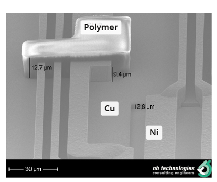
The figure shows the SEM image of the actuator structure of the microswitch made of nickel (electrolyte: NB Semiplate Ni 100). The narrow nickel bars were deposited on a sacrificial layer of copper (electrolyte: NB Semiplate Cu 100) with good thickness uniformity and high surface quality. The thickness of the sacrificial layer is approx. 3 µm. The overgrowth of the nickel structure over the edge of the sacrificial layer is clearly recognisable . The width of the nickel bars is around 4 µm, the edge steepness is almost 90°. Such conditions and requirements place high demands on the coating process, whereby a coating process with 18 µm AZ® 9260 at an aspect ratio of 4.5 with almost vertical side walls over a copper edge of approx. 3 µm was optimised here. The different levels of reflection of the substrates (copper sacrificial layer and gold start layer) require careful adjustment of the exposure parameters.
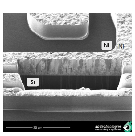
The image shows the sectional view of a structured nickel deposition (FIB section). The nickel was processed without brightener. The grain structure and the typical stem growth can be recognised at . The smaller grain structure in the lower layer area is also clearly recognisable, where the adaptation to the substrate takes place. In some applications special attention must be paid to this. Properties such as lustre, stress and grain growth can be influenced within certain limits by additives, but also by the process control. An admixture of Mn, for example, protects the grain structure from changes under mechanical or thermal stress. A fine grain structure can be preferred for narrow spring elements, as here with a width of 4 µm, but only if it is ensured that the grains are stable and do not enlarge or change under stress.
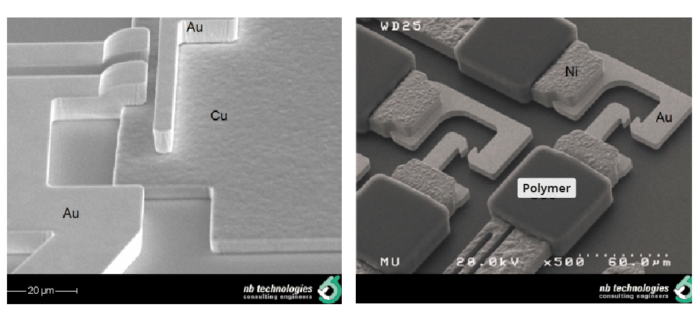
At the top left you can see an SEM image of a lateral microcontact made of gold(NB Semiplate Au 100) on a copper sacrificial layer(NB Semiplate Cu 100). The copper sacrificial layer shows very good thickness uniformity and surface quality. It is noteworthy that the higher roughness of the sacrificial layer, which is slight but recognisable , is levelled out again by the gold deposition .
The image on the top right shows the SEM image of the contact area of the microswitch. The contacts are made of bright gold(NB Semiplate Au 100). If necessary, the NB Semiplate Au 100 can be modified with a palladium additive (to NB Semiplate Au Pd 100) to improve the contact properties. The nickel of the thermal actuator(NB Semiplate Ni 100) is connected to the gold contact by overgrowth. The nickel is processed with low lustre with regard to the adhesive bond with the polymer. Nevertheless, a certain fineness of the grain size is processed with regard to the mechanical properties in the spring element with a small width of only 4 µm.
Multi-layer wiring on thin foils
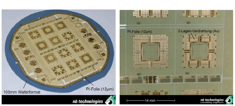
NB Semiplate Au 100 is used for the metallisation of multilayer wiring in conjunction with thin films. Shown here are 12 µm thick polyimide films with two metallisation layers. Special requirements exist here with regard to adhesion, layer stress, stability of properties and levelling of topographies.
